Photonic integrated circuit patents: how to claim a PIC
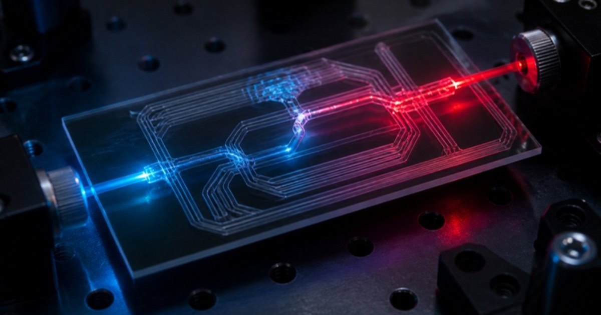
To get a strong photonic integrated circuit patent, claim the invention at three levels: the device structure you can see in a cross-section, the fabrication process that makes it, and the system that uses it. Each level protects against a different competitor, and each needs support in the specification you file on day one. One claim type alone usually leaves gaps.
This article is for silicon photonics founders and university lab researchers who have a new waveguide, modulator, coupler or laser integration scheme and want to know what to file. I cover what is patentable in a PIC, how to split claims between structure, process and system, a worked example of claiming a modulator design, timing around papers and conferences, and the mistakes I see most often. The aim is a filing that survives examination and still covers what competitors will actually build.
Key takeaways
- A photonic integrated circuit patent should usually include device claims, method-of-fabrication claims and system claims, because each one reaches a different infringer.
- Claim the structure that a competitor’s chip will show under cross-sectional imaging, not just the performance number from your paper.
- Functional results like “low loss” or “high bandwidth” need structural support, and broad claims need enough examples to enable their full scope.
- Process claims still matter when chips are made abroad, because U.S. law reaches imports of products made by a patented process.
- File before you publish, present or post a preprint. The U.S. one-year grace period does not protect you in Europe.
What can you patent in a photonic integrated circuit?
You can patent almost any new and non-obvious feature of a PIC: a waveguide geometry, a modulator doping profile, a grating or edge coupler, a laser bonding scheme, a fabrication sequence, a packaging method, or a system that combines these in a new way. The test is novelty and non-obviousness over prior art, not whether the physics is new.
Prior art means anything that was public before your filing date: earlier patents, journal papers, conference talks, product datasheets and even foundry design-kit documentation. Silicon photonics has decades of literature, so the question is rarely “is a microring modulator new?” It is “what about my microring, my junction or my process step is different, and why does it matter?”
Common patentable features in PIC work
- Passive structures: waveguide cross-sections, bends, tapers, spot-size converters, multimode interference couplers, grating couplers and polarization splitters.
- Active devices: carrier-depletion or carrier-injection phase shifters, electro-absorption modulators, thermo-optic heaters, germanium photodetectors and integrated lasers.
- Material platforms: thin-film lithium niobate, silicon nitride, indium phosphide and hybrid stacks. If your work is mostly about a new film or deposition chemistry, it may overlap with patent strategy for advanced materials.
- Processes: etch sequences, implant schedules, bonding and annealing steps, and wafer-level testing methods.
- Systems: transceivers, LiDAR engines, optical interconnects, sensors and photonic processors, including photonic approaches to quantum hardware.
The more specific your claims are to a real structural difference, the easier the examination. The broader they are, the more the specification has to carry.
How do you structure claims for a photonic integrated circuit patent?
A well-built photonic integrated circuit patent uses three claim families. Device claims cover the chip as a physical object. Method claims cover how it is made. System claims cover the product a customer buys. Together they let you pursue the foundry, the chip vendor and the module or system maker, depending on who is doing what.
A claim is the numbered sentence at the end of a patent that defines what you own. An independent claim stands alone. A dependent claim adds limits to an earlier claim, which gives you fallback positions if the broad claim is challenged.
| Claim type | What it covers | Who it reaches | Main risk |
|---|---|---|---|
| Device (structure) | The waveguide, modulator or circuit as built: layers, dimensions, doping, geometry | Anyone who makes, uses, sells or imports the chip | Prior art with a similar cross-section; design-arounds that change one dimension |
| Method of fabrication | The sequence of deposition, lithography, etch, implant and anneal steps | Foundries and integrated device makers; importers of chips made by the method | Hard to detect from the finished chip; process often owned by the foundry |
| System | The transceiver, LiDAR unit or sensor that includes the PIC | Module makers and system integrators | Easier to design around by changing a non-photonic part; may be seen as an obvious combination |
| Method of operation | How the device is driven, tuned or calibrated in use | Users and makers of control electronics or firmware | Infringement may be spread across several parties |
Not every invention needs all four. A new grating coupler may be best protected with device and fabrication claims. A new calibration method for a phased array may be mostly operation and system claims. The point is to decide on purpose rather than by default.
Why claim the device structure first?
Structure claims are usually the most valuable because infringement can be shown from the product itself. A competitor’s chip can be cross-sectioned and imaged, and its layer stack, etch depth and doping regions measured. If your claim recites those features, you can prove infringement without access to anyone’s fab records.
This is where my science training changes how I draft. I ask what a failure-analysis lab would see in a competitor’s die. A rib waveguide’s slab thickness, the lateral offset of a PN junction from the waveguide center, the gap in a directional coupler and the period of a grating are all visible. An internal process temperature is not.
Write structure, not just results
A paper often leads with a result: insertion loss, modulation efficiency, bandwidth or footprint. Those results matter, but a claim built only on them is risky. U.S. law requires claims that particularly point out and distinctly claim the invention, and a specification with a written description and enabling instructions for the full scope claimed, under 35 U.S.C. § 112.
Words of degree such as “low loss” or “substantially uniform” are not automatically indefinite. The USPTO’s guidance in MPEP § 2173 says the examiner should check whether the specification provides some standard for measuring that degree. So if you use such a term, define it in the specification with a number, a measurement method and a wavelength.
Breadth needs examples
Founders often want a claim that covers “any modulator that achieves X.” The Supreme Court addressed this kind of claim in Amgen Inc. v. Sanofi (2023), a unanimous decision that stated, “The more one claims, the more one must enable.” The case involved antibodies, but the principle applies to any technology. If you claim a whole class of geometries defined by a performance target, your application needs enough examples, design rules or simulation data to teach how to make the full class.
How should you claim the fabrication process?
Claim the fabrication process when the process itself is new, such as a self-aligned implant, a two-step partial etch or a low-temperature bonding sequence. Process claims are harder to police because the steps are hidden inside the fab, but they reach foundries directly and, under U.S. law, can reach imported chips made by the claimed process.
That second point matters because many PIC startups use foundries outside the United States. Under 35 U.S.C. § 271(g), whoever imports into, or sells or uses within, the United States a product made by a process patented in the United States can be liable as an infringer. There are exceptions, including when the product is materially changed by later processes or becomes a trivial and nonessential component of another product.
Product-by-process claims
Sometimes the only clear way to describe a structure is by how it was made, for example “a waveguide sidewall formed by a hydrogen anneal.” This is a product-by-process claim. Under MPEP § 2113, patentability is based on the product itself, not the method of production, although the structure implied by the process steps should be considered. If a prior-art waveguide has the same structure, a new process will not save a product-by-process claim. Describe the resulting structure, such as a measured sidewall roughness, wherever you can.
Foundry design kits and who owns the process
If you design on a foundry’s process design kit, the base process belongs to the foundry. Your invention is usually in the layout, the device design or a modification you specified. Read your foundry agreement before filing. It may limit what you can claim, require notice, or give the foundry rights in process improvements made on its line.
Worked example: claiming a silicon modulator design
Here is a hypothetical showing how the three levels fit together. Suppose your lab built a carrier-depletion phase shifter for a Mach-Zehnder modulator in silicon-on-insulator. The rib has a PN junction offset from its center, plus a narrow, more heavily doped strip near the junction that improves modulation efficiency without the loss penalty of doping the whole rib.
The facts below are invented for illustration. They are not drawn from any real application or client matter.
Step 1: Find the structural core
Ask what makes the device work and what a competitor would have to copy to get the same result. In this example, the core is the combination of the junction offset and the heavily doped strip at a defined position relative to the junction. The specific doping numbers are useful, but they belong in dependent claims.
Step 2: Draft the independent device claim
A simplified version might read:
1. An optical phase shifter comprising: a silicon rib waveguide having a rib and a slab on an insulator layer; a p-type region and an n-type region within the rib that meet at a PN junction, the PN junction being laterally offset from a center line of the rib; and a doped strip within the rib adjacent the PN junction, the doped strip having a dopant concentration higher than a dopant concentration of the adjacent p-type or n-type region and a width less than half a width of the rib.
Notice what is in it: layers, regions, positions and a relative width. Notice what is not: a bandwidth number, a wavelength or a specific foundry process. Every element can be measured on a finished chip.
Step 3: Build dependent claims as fallbacks
- The rib height and slab thickness ranges you actually tested.
- Dopant concentration ranges for the strip and the surrounding regions.
- The lateral offset of the junction as a range or a fraction of the rib width.
- A traveling-wave electrode arrangement for the Mach-Zehnder arms.
- Alternative materials, such as a silicon nitride or thin-film lithium niobate version, if your data supports them.
If an examiner finds a paper close to claim 1, these give you room to narrow without starting over.
Step 4: Add a fabrication method claim
If you developed a self-aligned way to place the doped strip, for example using a hard mask edge to define both the rib and the implant window, claim that sequence as a method. Be ready for a restriction requirement. Under MPEP § 806.05(f), an examiner can treat a process of making and the product made as distinct inventions if the product can be made by another materially different process. You may have to elect one and pursue the other in a divisional application.
Step 5: Add a system claim
Finally, claim an optical transceiver or interconnect that includes the modulator, a laser source and a driver circuit. This claim reaches the module maker even if the chip vendor is outside the United States. Keep the system claim tied to the new phase shifter. A claim that only adds standard parts may be rejected as obvious.
Step 6: Support it all in the specification
Include cross-section drawings, a table of the dimensions and doping levels you built, simulation results across the claimed ranges and at least one alternative embodiment. If you claim a range, show why the end points make sense. This is the material that holds the claims up during examination and later in litigation.
When should you file a PIC patent application?
File before any public disclosure: a journal paper, conference talk, poster, preprint, investor deck shared without a confidentiality agreement, or a product sample. The United States gives inventors a one-year grace period for their own disclosures. Europe and many other jurisdictions do not, so a paper published first can cost you foreign rights.
Under 35 U.S.C. § 102(b)(1)(A), a disclosure made one year or less before the effective filing date is not prior art if the inventor made it. In Europe, Article 54 of the European Patent Convention treats everything made available to the public before the filing date as part of the state of the art. There is no general one-year inventor exception like the U.S. one.
For university labs, the usual fix is a provisional application filed shortly before the paper goes out. A provisional application is a U.S. filing that holds your priority date for 12 months, but only for what it actually describes. A provisional that is just the paper, with no claims and no alternatives, often protects less than people think. I go through this timing in more detail in when to file and why the clock starts earlier than you think.
What mistakes weaken a photonic integrated circuit patent?
The most common mistakes are claiming only performance, claiming only what a foundry can see, filing a thin provisional before a paper, and ignoring who will actually infringe. Each one can leave a granted photonic integrated circuit patent that looks impressive but is hard to enforce or easy to design around.
A pre-filing checklist
- List every structural feature that is new, and mark which ones can be measured on a finished chip.
- Note any process step that is new, and whether it is yours or the foundry’s.
- Identify who would infringe each claim type: foundry, chip vendor, module maker or end user.
- Collect the ranges you tested and any simulations that extend them.
- Gather at least one alternative embodiment for each key feature, such as another material platform or geometry.
- Check publication, conference and preprint dates, and plan the filing before the first one.
- Review foundry, university and grant agreements for ownership and reporting terms.
- Decide whether foreign filing matters for your market, since that affects whether any public disclosure is acceptable.
Investors will ask many of the same questions during diligence. If you are raising a round, my post on what investors ask about your patents covers how they look at claim scope and ownership. Spin-outs face added steps around university licensing, which I discuss on the startups and university spin-outs page.
For more on the kinds of optical and photonic work I handle, see my photonics and optics patent practice.
Frequently asked questions
Can I patent a photonic integrated circuit made on a standard foundry process?
Yes, if your design adds something new and non-obvious. Most PIC startups use a foundry process and patent the device layout, geometry, doping arrangement or circuit architecture they created on top of it. You generally cannot claim the foundry’s base process as your own. Check your foundry agreement for terms on improvements and confidentiality before you file.
Should I patent the device or the fabrication method?
Usually both, if both are new. Device claims are easier to enforce because infringement can be shown by imaging a competitor’s chip. Method claims reach foundries and, under 35 U.S.C. § 271(g), can reach imports of chips made by the patented process. If only one is new, put your effort there and claim the other only if the specification supports it.
Can I publish a paper before filing a patent application?
In the United States, your own disclosure is not prior art against you if you file within one year. In Europe and many other countries, anything public before the filing date counts as prior art. The safer path is to file at least a provisional application before the paper, talk or preprint becomes public.
How broad can my waveguide or modulator claims be?
As broad as the prior art allows and your specification supports. A claim defined only by a performance target, such as any modulator above a certain bandwidth, needs enough examples and design guidance to enable that whole scope. The safer approach is a structural independent claim with dependent claims that narrow to the dimensions and doping levels you tested.
Is a provisional application enough to protect my PIC invention?
A provisional holds your filing date for 12 months, but only for what it describes. If it is just a draft paper, later claims to alternatives or broader ranges may not get the earlier date. Include cross-sections, the structural features you consider key, tested ranges and alternative embodiments, so the nonprovisional application can rely on it.
If you are deciding whether to file before a conference, a paper or a fundraise, I am happy to talk it through.
This article is general information, not legal advice, and reading it does not create an attorney-client relationship. Patent law changes and every situation differs. Please talk to a patent attorney about yours.